

Transport in nanoelectronic materials and devices
Behind the current versus voltage characteristics of any semiconductor device, there is a transport problem describing how electrons are injected at some electrodes and collected at some other electrodes. Electrons in the semiconductors are driven by the electric (and magnetic) field, and the electrostatic potential is in turn affected by the carrier densities. Hence the transport and electrostatics equations usually must be solved self-consistently, which demands a numerical approach. The geometrical scaling of the devices and the development of 3-D device architectures has further complicated the picture, in that the tiny device features result in size-induced quantization effects. Moreover, quantum effects can occur also in the transport direction, both in MOSFETs and in tunnelling devices.
For more than twenty years our group has been engaged in numerical models for electronic transport in nanoelectronics materials and devices. Our expertise covers TCAD commercial tools, as well as the in-house development of our own simulators. We have developed electron device simulation tools based on the semi-classical Boltzmann Transport Equation (BTE) solved with either statistical methods (e.g. the Monte Carlo approach) or deterministic methods, and for device architectures ranging from conventional bulk MOSFETs to nanowire and nanosheet Gate All Around FETs.
More recently we have extended our know-how to quantum transport based on the Non Equilibrium Green’s Function (NEGF) method, in collaboration with Marco Pala. The Hamiltonian models that can be used in our NEGF simulations range from a simple effective mass approximation approach, to the Density Functional Theory (DFT) Hamiltonians employed in the ab-initio solver Quantum ESPRESSO. The computational burden increases dramatically when moving towards more physically sound models, which makes it necessary the use of High Performance Computing resources.
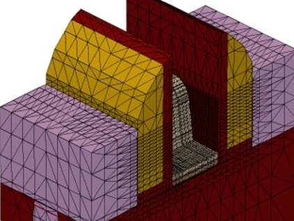
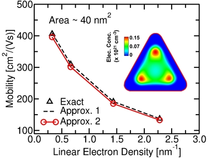
Improved surface-roughness scattering and mobility models for multi-gate FETs with arbitrary cross-section and biasing scheme
D. Lizzit, O. Badami, R. Specogna, D. Esseni, Journal of Applied Physics, vol. 121, 245301, 2017. doi: 10.1063/1.4986644
A new formulation for surface roughness limited mobility in bulk and ultra-thin-body metal–oxide–semiconductor transistors
D. Lizzit, O. Badami, R. Specogna, D. Esseni, Journal of Applied Physics, vol. 116, 223702, 2014. doi: 10.1063/1.4986644
On the origin of the mobility reduction in n- and p-metal-oxide-semiconductor field effect transistors with hafnium-based/metal gate stacks
P. Toniutti, P. Palestri, D. Esseni, F. Driussi, M. De Michielis, L. Selmi, Journal of Applied Physics, vol. 112, p. 034502, 2012. doi: 10.1063/1.4737781
Investigation of the transport properties of silicon nanowires using deterministic and Monte Carlo approaches to the solution of the Boltzmann Transport Equation
M. Lenzi, P. Palestri, E. Gnani, S. Reggiani, A. Gnudi, D. Esseni, L. Selmi, G. Baccarani, IEEE Transactions on Electron Devices, vol. 55, p. 2086-2096, 2008, doi: 10.1109/TED.2008.926230
Multi-Subband Monte-Carlo study of Transport, Quantization and Electron Gas Degeneration in Ultra-Thin SOI n-MOSFETs
L. Lucci, P. Palestri, D. Esseni, L. Bergagnini, L. Selmi. IEEE Transactions on Electron Devices, vol. 54, p. 1156-1164, 2007
On the Modeling of Surface Roughness Limited Mobility in SOI MOSFETs and its Correlation to the Transistor Effective Field
D. Esseni, IEEE Transactions on Electron Devices, vol. 51, p. 394-401, 2004.
Modeling of electron mobility degradation by remote Coulomb scattering in ultrathin oxide MOSFETs
D. Esseni and A. Abramo, IEEE Transactions on Electron Devices, vol. 50, p. 1665-1674, 2003. doi: 10.1109/TED.2003.814973
Physically Based modeling of Low Field Electron Mobility in Ultrathin Single- and Double-Gate SOI n-MOSFETs
D. Esseni, A. Abramo, L. Selmi, E. Sangiorgi. IEEE Transactions on Electron Devices, vol. 50, p. 2445-2455, 2003. ISSN: 0018-9383, doi: 10.1109/TED.2003.819256
Selected publications about quantum transport
Full-Band Quantum Transport of Heterojunction Electron Devices with Empirical Pseudopotentials
A. M'Foukh, M. Pala, D. Esseni, IEEE Transactions on Electron Devices, vol. 67, p. 5662-5668, 2020. doi: 10.1109/TED.2020.3029548.
Unit cell restricted Bloch functions basis for first-principle transport models: Theory and application.
M. Pala, P. Giannozzi, D. Esseni. Physical Review B, vol. 102, pp. 045410, 2020 doi: 10.1103/PhysRevB.102.045410.
Quantum transport models based on NEGF and empirical pseudopotentials for accurate modeling of nanoscale electron devices
M. Pala, D. Esseni, Journal of Applied Physics, vol. 126, pp. 055703, 2019. doi: 10.1063/1.5109187
Full-band quantum simulation of electron devices with the pseudopotential method: Theory, implementation, and applications
M. Pala and D. Esseni, Physical Review B, vol. 97, 125310, 2018, doi: 10.1103/PhysRevB.97.125310
Operation and Design of van der Waals Tunnel Transistors: A 3-D Quantum Transport Study
J. Cao, D. Logoteta, S. Ozkaya, B. Biel, A. Cresti, M. Pala, D. Esseni, IEEE Transactions on Electron Devices, vol. 63, p. 4388-4394, 2016. doi: 10.1109/TED.2016.2605144
Strain-Induced Performance Improvements in InAs Nanowire Tunnel FETs
F. Conzatti, M. Pala, D. Esseni, E. Bano, L. Selmi, IEEE Transactions on Electron Devices, vol. 59, p. 2085-2092, 2012. doi: 10.1109/TED.2012.2200253