
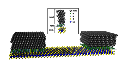

Quasi 2-D materials and related devices
Graphene has been the first two-dimensional (2-D) material to be discovered and led to the Nobel price for physics in 2010. Then, several atomically thin 2-D semiconductors belonging to the family of transition metal dichalcogenides (TMDs) were reported, which exhibit interesting electronical and optical properties. In particular, thanks to their extreme flexibility and large piezo-resistance, TMDs like MoS2 have great prospective applications ranging from fast thermal and pressure sensors, to tactile sensing in soft robotics and electronic skin. Moreover, TMDs have attracted remarkable attention for beyond silicon CMOS circuits. In fact, the scaling of silicon based FETs to channel lengths in the sub 10-nanometer range appears very problematic, and single-layer TMDs have been identified as promising baseline materials for ultimately scaled FETs, thanks to a combination of sub-nanometer thickness, fairly large energy bandgap, and good electronic mobility compared to conventional semiconductors at comparable layer thickness.
Our group has been involved in several activities related to graphene and 2-D semiconductors, for applications ranging from strain and pressure sensors to advanced transistors and optoelectronic devices. These activities have been carried in the framework of projects funded by the European Union (GRADE, GA: 317839 and GRAND, GA: 215752), and more recently in the framework of the PRIN project FIVE2D (number 2017SRYEJH) funded by the Italian MIUR.
Sub-60mV/dec Swing and Drive Current in Dirac-Source FETs: A Design Study Based on First-Principle Transport Simulations
D. Nguyen, A. Pilotto, D. Lizzit, M. Pala and D. Esseni, "Sub-60mV/dec Swing and Drive Current in Dirac-Source FETs: A Design Study Based on First-Principle Transport Simulations," IEEE International Electron Devices Meeting (IEDM), San Francisco, 2024
Reinterpreting Low Resistance in Sb–MoS2 Ohmic Contacts by Means of Ab Initio Transport Simulations
D. Lizzit, M. Pala, F. Driussi and D. Esseni, "Reinterpreting Low Resistance in Sb–MoS2 Ohmic Contacts by Means of Ab Initio Transport Simulations, IEEE Transactions on Electron Devices, vol. 71, no. 5, pp. 3301-3306, 2024.
Ohmic Behavior in Metal Contacts to n/p-Type Transition-Metal Dichalcogenides: Schottky versus Tunneling Barrier Trade-off
Daniel Lizzit, Pedram Khakbaz, Francesco Driussi, Marco Pala, and David Esseni, ACS Applied Nano Materials 6 (7), 5737-5746, 2023
Ab–initio transport simulations unveil the Schottky versus Tunneling barrier trade–off in metal–TMD contacts
D. Lizzit, P. Khakbaz, F. Driussi, M. Pala, and D. Esseni, Proceedings of International Electron Devices Meeting (IEDM), 2022.
Large temperature coefficient of resistance in atomically thin two-dimensional semiconductors
A. I. Khan, P. Khakbaz, K. A. Brenner, K. K. H. Smithe, M. J. Mleczko, D. Esseni, E. Pop. Applied Physics Letters, vol. 116, 203105, 2020.
Piezoresistive Properties of Suspended Graphene Membranes under Uniaxial and Biaxial Strain in Nanoelectromechanical Pressure Sensors
A. D. Smith, F. Niklaus, A. Paussa, S. Schröder, A.C.Fischer, M. Sterner, S. Wagner, S. Vaziri, F. Forsberg, D. Esseni, M. Östling, Max C. Lemme, ACS Nano, vol. 10, p. 9879-9886, 2016.
Strain-Induced Modulation of Electron Mobility in Single-Layer Transition Metal Dichalcogenides MX2 (M = Mo, W; X = S, Se)
M. Hosseini, M. Elahi, M. Pourfath, D. Esseni, IEEE transactions on Electron Devices, vol. 62, p. 3192-3198, 2015.
Two-Dimensional Heterojunction Interlayer Tunneling Field Effect Transistors (Thin-TFETs).
M. Li, Mingda, D. Esseni, J. J. Nahas, D. Jena, H. G. Xing, IEEE Journal of the Electron Devices Society, vol. 3, p. 200-207, 2015.
Electromechanical Piezoresistive Sensing in Suspended Graphene Membranes
A. D. Smith, F. Niklaus, A. Paussa, S. Schröder, S. Vaziri, A.C. Fischer, M. Sterner, A.Delin, D. Esseni, P. Palestri, M. C. Lemme, Nano Letters, vol. 13, p. 3237-3242, 2013.
Simulation of the Performance of Graphene FETs With a Semiclassical Model, Including Band-to-Band Tunneling
A. Paussa, G. Fiori, P. Palestri, M. Geromel, D. Esseni, G. Iannaccone, L. Selmi, IEEE Transactions on Electron Devices, vol. 61, p. 1567-1574, 2014.