

Advanced CMOS FETs
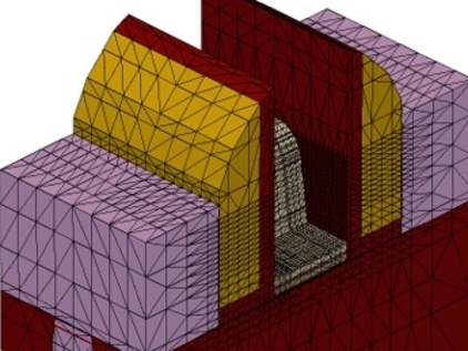
Bulk planar transistors were fabricated in a semiconductor substrate very deep compared to the thin, interfacial region where carrier transport actually takes place. Bulk transistor have been the transistor architecture for CMOS integrated circuits for some decades, and have undergone an impressive miniaturization process, known as scaling. In the last decade, however, in the attempt to overcome the scaling limits of bulk MOSFETs, CMOS technology has rapidly evolved from bulk devices to silicon on insulator (SOI) transistors realized in ultra-thin semiconductor layers (UTB-FETs), that can be operated either in single or in double gate mode. Then a progressive evolution towards three-dimensional (3-D) transistor architectures occurred. FinFETs were first demonstrated around year 2000, then in 2012 Intel reported on a leading edge 22nm CMOS technology featuring 3-D Tri-Gate MOSFETs for logic applications [31], and in 2014 announced its new 14-nm technology node FinFET featuring a 20 nm gate length, 8 nm fin width and 42 nm fin height. As an evolution towards 3-D transistors, gate all around nanowire MOSFETs are the most promising architectures for ultimate device scaling, because they allow for an almost ideal gate control on the channel region, which is completely surrounded by the gate.
In this framework, our group has developed numerical models and carried out design studies for several flavours of nanoscale transistors ranging from planar to 3-D architectures, to FinFETs, NanoWire FETs and Nano-Sheet FETs. These activities about advanced CMOS architectures and new chanel materials have been developed in the framework of a collaboration with TSMC Europe, and of the project III-V-MOS (FP7, GA:619326) funded by the European Union.
Benchmarking of 3-D MOSFET Architectures: Focus on the Impact of Surface Roughness and Self-Heating
O. Badami, D. Lizzit, F.Driussi, P. Palestri, D. Esseni, IEEE Transactions on Electron Devices, vol. 65, p. 3646-3653, 2018.
An Improved Surface Roughness Scattering Model for Bulk, Thin-Body, and Quantum-Well MOSFETs
O. Badami, E. Caruso, D. Lizzit, P. Osgnach, D. Esseni, P. Palestri, L. Selmi, IEEE Transactions on Electron Devices, vol. 63, p. 2306-2312, 2016.
Performance Benchmarking and Effective Channel Length for Nanoscale InAs, In0.53Ga0.47As, and sSi n-MOSFETs
D. Lizzit, D. Esseni, P. Palestri, P. Osgnach, L. Selmi, IEEE Transactions on Electron Devices, vol. 61, p. 2027-2034, 2014.
Analysis of the Performance of n-Type FinFETs With Strained SiGe Channel
D. Lizzit, P. Palestri, D. Esseni, A. Revelant, L. Selmi, IEEE Transactions on Electron Devices, vol. 60, p. 1884-1891, 2013.
Mixed FBB/RBB: A Novel Low-Leakage Technique for FinFET Forced Stacks
D. Baccarini, D. Esseni, M. Alioto M. (2012). IEEE Transactions on Very Large Scale Integration (VLSI) Systems, vol. 20, p. 1467-1472, 2012.
A Quantitative Error Analysis of the Mobility Extraction According to the Matthiessen Rule in Advanced MOS Transistors
D. Esseni, F. Driussi, IEEE Transactions on Electron Devices, vol. 58, p. 2415-2422, 2011.
Mobility Enhancement in Strained n-FinFETs: Basic Insight and Stress Engineering
N. Serra, D. Esseni, IEEE Transactions on Electron Devices, vol. 57, p. 482-490, 2010.
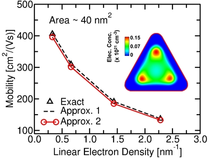
Investigation of the transport properties of silicon nanowires using deterministic and Monte Carlo approaches to the solution of the Boltzmann Transport Equation
M. Lenzi, P. Palestri, E. Gnani, S. Reggiani, A. Gnudi, D. Esseni, L. Selmi, G. Baccarani. IEEE Transactions on Electron Devices, vol. 55, p. 2086-2096, 2008.
Understanding Quasi-Ballistic Transport in nano-MOSFETs. Part I:Scattering in the Channel and in the Drain
P. Palestri, D. Esseni, S. Eminente, C. Fiegna, E. Sangiorgi, L. Selmi, IEEE Transactions on Electron Devices, vol. 52, p. 2727-2735, 2005.